Benefits from
Mask-less Circuit Printing
We want to give you the freedom
to 3D print high-resolution
or very thick electronic
circuits, bumps and bonding
layers through the AMEBA 3D
(S-ECAM for 3D Circuit) series
of machines.
01
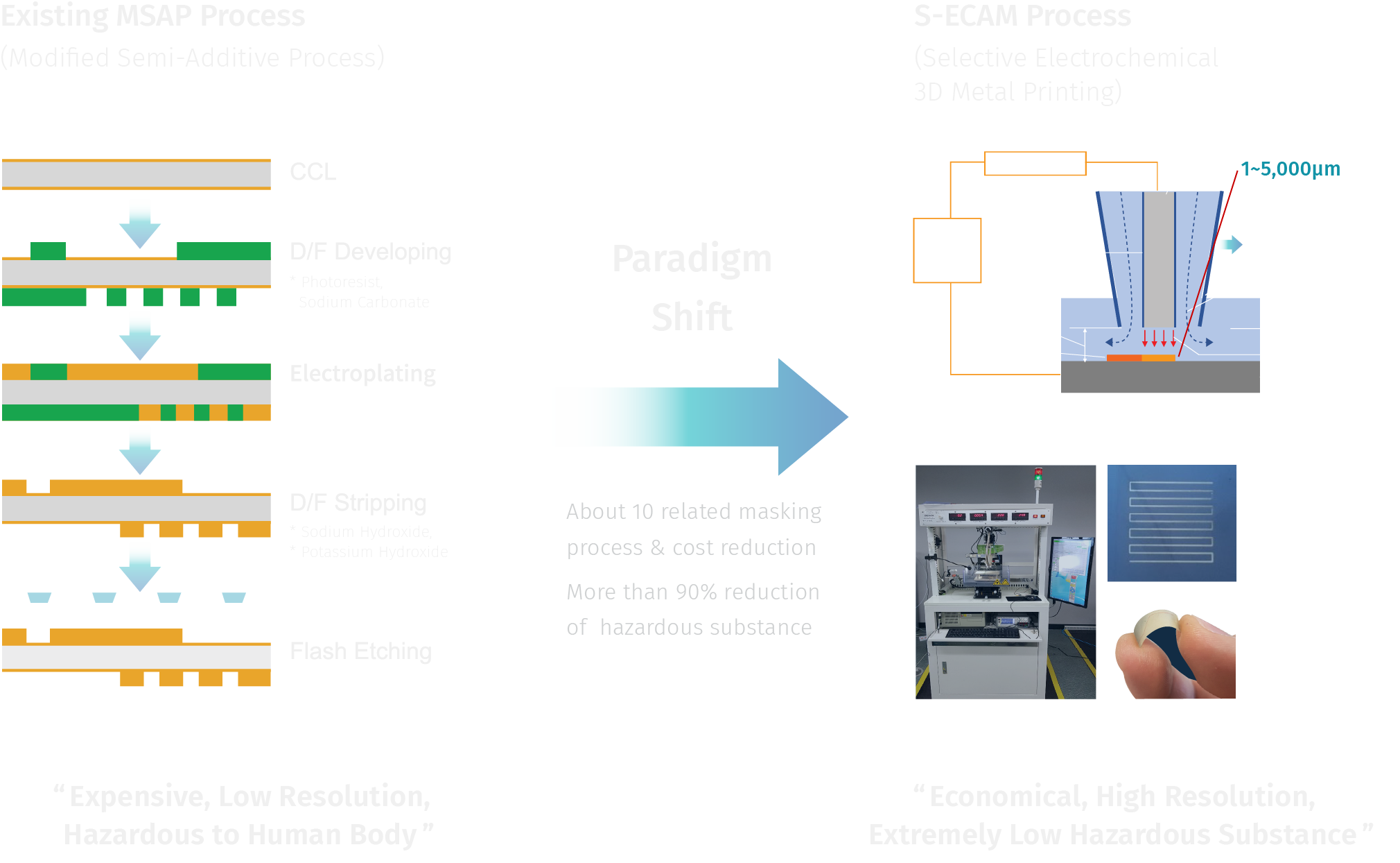
S-ECAM will be able to replace some of the existing SAP (Semi-Additive Process) and MSAP (Modified SAP) processes with a mask-less metal printing process, which will be the beginning of the paradigm shift. It can reduce more than 10 processes and costs related to masking process and can reduce harmful substances by more than 90%. S-ECAM can also print circuits of higher resolution more economically.
02
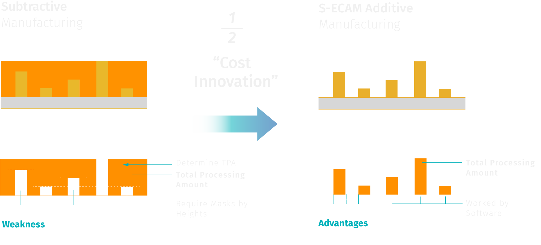
When manufacturing wafer bumps with a thickness of 50 ~ 200 ㎛ for normal semiconductors, or patterns with a thick
ness of 10 ~ 5,000 ㎛ for high-power semiconductors, if the subtractive manufacturing is performed by the wet etching
method, the Total Processing Amount (TPA) is significantly increased, and complex and expensive masking process
should be involved. Conversely, if the additive manufacturing is performed using S-ECAM, the TPA is greatly reduced,
the masking process can be eliminated, and extremely small line & space can be obtained.
To manufacture wafer bump with the MSAP Modified Semi Additive Process, the 7 equipment and peripheral
devices such as Asher, Laminator, Lithographer, Developer, Striper, Etching, Electroplating are required. It is estimated
that the cost for equipment investment is about USD 2.4 Mil. and the operating cost is about 0.2 Mil. In comparison, the
use of S-ECAM can reduce the cost of equipment and peripherals to about USD 1.1 Mil and operating cost to about USD
0.03 Mil, and the sum of these two costs is less than half that of MSAP.